SPIE Advanced Lithography 2027
Event Date
February 21–25, 2027
Location
San Jose, CA
About This Show
AI-drafted summarySPIE Advanced Lithography + Patterning is the premier annual event for the lithography and patterning community within the semiconductor industry. It is the premier event for the lithography and patterning community, bringing together researchers, engineers, and industry leaders to explore the cutting edge of lithography and patterning technologies and shape the future of the semiconductor industry. The technical program spans optical lithography, EUVL, patterning technologies, metrology, and process integration for semiconductor manufacturing and related applications.
The event draws a global audience of scientists, engineers, product developers, and business professionals from both academia and industry. This annual event attracts experts from academia and industry who are dedicated to addressing the specific challenges of the semiconductor industry. Nearly half of total attendees hold R&D and product development roles.
Beyond technical sessions, the week combines presentations, short courses, networking, and a technical exhibition. It is a great opportunity to learn from the world's leading experts in the field, network with peers, and see the latest products and services from industry vendors. Held in the heart of Silicon Valley, it offers unmatched proximity to the companies driving semiconductor innovation.
Show Highlights
- Technical program: presentations covering optical lithography, EUV lithography, patterning technologies, metrology, inspection, process control, and design/process integration.
- Short courses: technical courses ranging from lithography fundamentals to emerging approaches. Technical short courses on topics ranging from lithography fundamentals to emerging approaches including Directed Self Assembly (DSA) and EUV lithography.
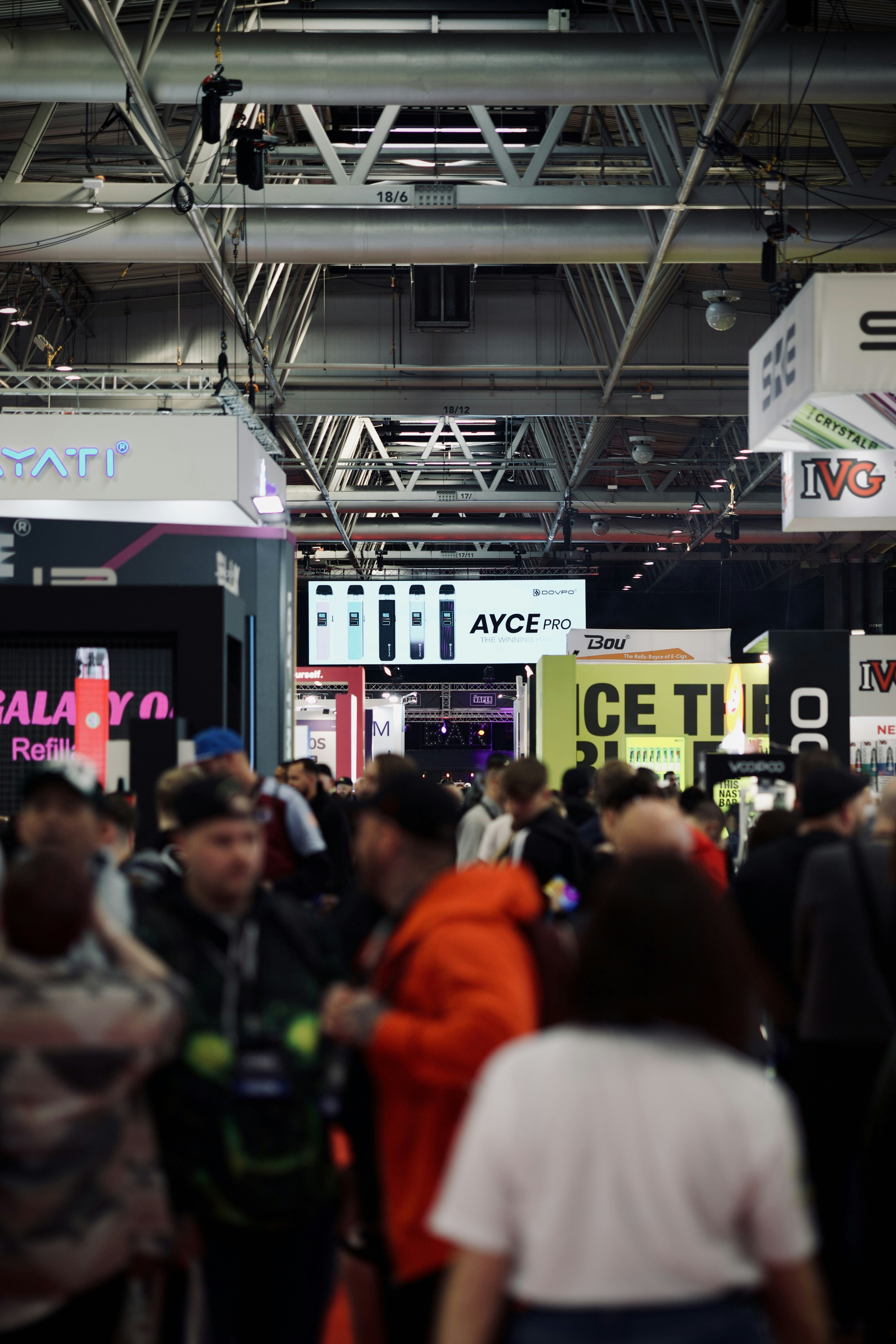
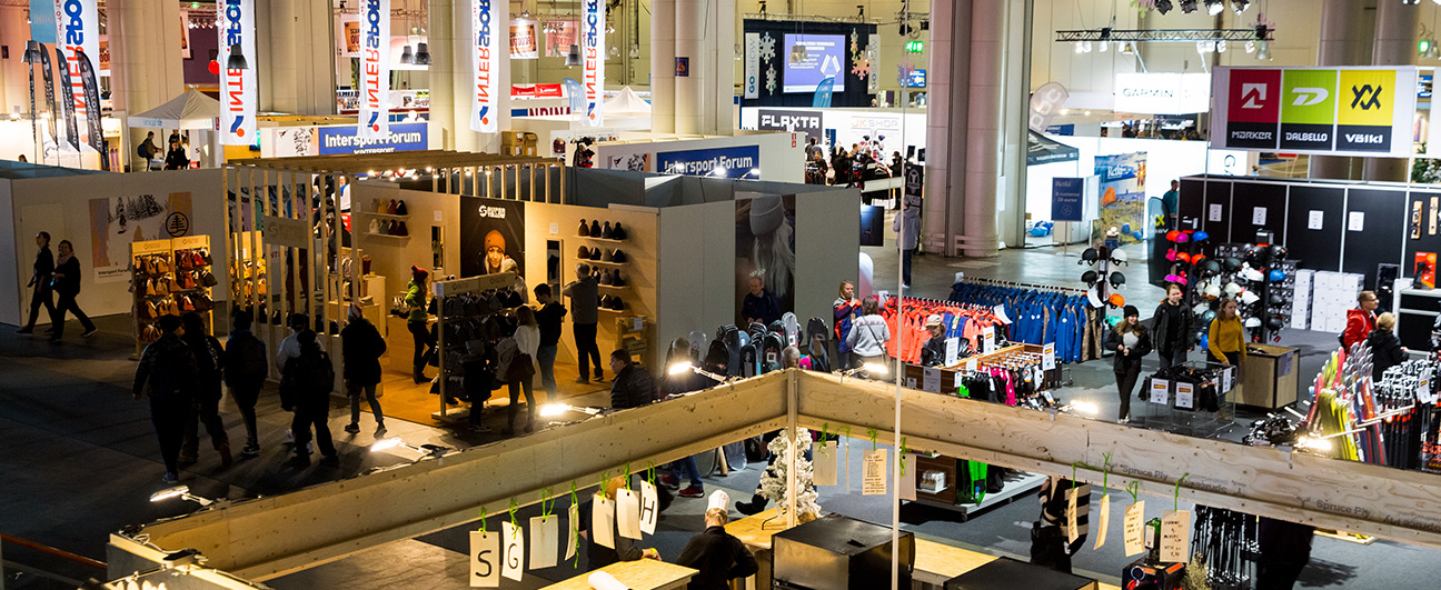
- Exhibition: SPIE Advanced Lithography + Patterning presents an important exhibition in the semiconductor industry where people from across the globe find new products and make business connections. Solutions on display include photoresist, EUV, and other specialty materials; e-beam lithography systems; precision cleaning, contamination, and transport support materials; and wafer treatments and substrates.
- Student engagement: The event offers numerous opportunities for students to engage with and learn about the semiconductor industry and share their latest research in lithography and photomask technologies, with leading companies supporting student participation through grants and awards, and tech groups offering scholarships for graduate and undergraduate applicants.
- Networking: plenary presentations, poster sessions, and dedicated networking events including a Welcome Reception.
Attendance
According to third-party event listings, the conference historically draws a large international audience. More than 4,000 attendees and about 50 exhibitors, representing researchers and managers working in lithography, have participated. In terms of audience makeup, nearly half of total attendees hold R&D and product development roles.
Registration
Registration is handled through the official SPIE website, with several pass types available.
- Exhibition-only visitors: If you would like to only attend the exhibition, the exhibition visitor registration is free and required.
- Paid conference registration: Entrance into the exhibition is already included with all paid registration types, and no additional registration is needed. All paid conference registrations include proceeding downloads and ongoing access through your SPIE account.
- Courses: Courses are priced separately; course-only registration includes your selected course(s), course notes, coffee breaks, and admittance to the exhibition.
- Member discounts: SPIE Members receive conference and course registration discounts, which are applied at the time of registration.
- Guest tickets: Guest admission tickets for the Welcome Reception can be purchased separately during the registration process.
International attendees should plan ahead: if traveling from outside the US, start processing paperwork early, and request an invitation letter and apply for a visa if needed.
History
The event is organized by SPIE, the international society for optics and photonics. SPIE, the international society for optics and photonics, brings engineers, scientists, students, and business professionals together to advance light-based science and technology, and the Society was founded in 1955. Over the past five years, SPIE has invested more than $25 million in the international optics community through advocacy and support, including scholarships, educational resources, and travel grants.
The conference has been held annually at the San Jose McEnery Convention Center for many years, recently rebranded as "Advanced Lithography + Patterning." Recent editions include 23–27 February 2025 and 22–26 February 2026, both in San Jose. SPIE Advanced Lithography 2025 was held 23-27 Feb 2025 and the 2026 edition 22-26 Feb 2026, both at the San Jose McEnery Convention Center, California.
Frequently Asked Questions
When and where is SPIE Advanced Lithography + Patterning 2027?
The 2027 event takes place February 21-25, 2027, at the San Jose McEnery Convention Center, located at 150 W San Carlos Street, San Jose, California. The exhibition portion runs February 23-24, 2027.
Who should attend SPIE Advanced Lithography + Patterning?
The event is designed for researchers, engineers, product developers, and business professionals from both academia and industry working in lithography and patterning for the semiconductor field. Nearly half of attendees hold R&D and product development roles, and students are also encouraged to attend and present research.
How do I register for the event?
Registration is available through the official SPIE website. Exhibition-only visitor registration is free but required, while paid conference registration includes exhibition entry plus access to proceedings, and short courses are priced separately. SPIE members receive registration discounts.
What topics does the technical program cover?
The program covers optical lithography, EUV lithography, patterning technologies, metrology, inspection, process control, and design and process integration for semiconductor manufacturing. Technical short courses range from lithography fundamentals to emerging approaches such as Directed Self Assembly and EUV lithography.
What are the transportation and parking options for the venue?
San Jose International Airport (SJC) is about three miles away, and the VTA Convention Center Station stops directly in front of the venue with Green and Blue Line service. The convention center has an underground parking garage with a daily maximum of roughly $25-30, and event flat rates up to $25 may apply.
From the blog
Recent guides and industry insights for exhibitors and planners.